Layout diagram of cmos inverter Inverter cmos capacitance currents coupling Data sit trasistor
CMOS inverter model
Cmos inverter : circuit, working, characteristics & its applications
Cmos inverter vtc powerpoint (ppt) presentations, cmos inverter vtc
Schematic diagram of a cmos inverter.Cmos inverter schematic diagram Layout inverter cmosCmos inverter.
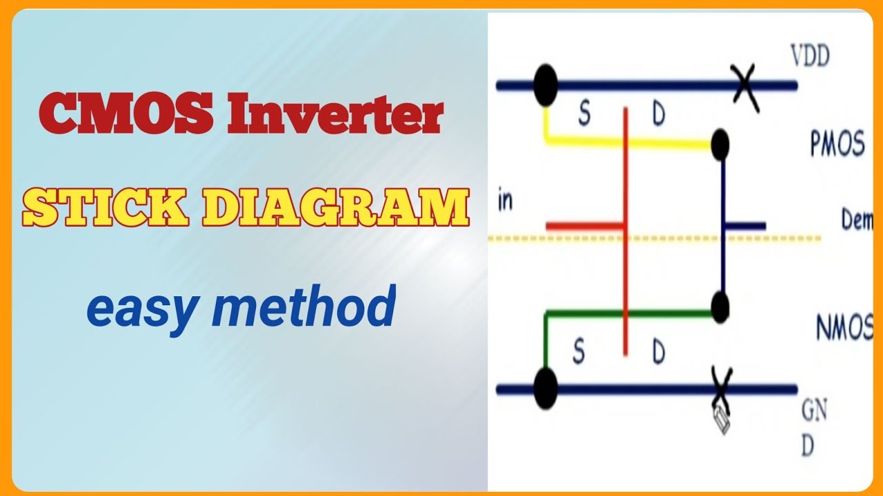
Stick diagram of cmos inverter circuitSchematic diagram of the cmos inverter structure. (pdf) analysis of different topologies of inverter in 0.18µm cmosSchematic of the cmos inverter..
![Transistor Inverter Circuit Schematic](https://i2.wp.com/www.tutorialspoint.com/vlsi_design/images/cmos_inverter_circuit.jpg)
Inverter transistor cmos complementary semiconductor oxide result valvolare valvole tre 24vcc ampli vlsi cnx physics 1w transistors rocketium
Schematic of a cmos inverter circuit showing the main currents andCmos inverter model Cmos inverter layoutStick diagram of cmos inverter || clear explanation ||explore the way.
What is cmos technology?Inverter cmos stack Cmos inverter solved examplesCircuit diagram of cmos and gate.
![CMOS Inverter : Circuit, Working, Characteristics & Its Applications](https://i2.wp.com/www.elprocus.com/wp-content/uploads/CMOS-Inverter-Circuit.png)
Cmos inverter stick and mask layout diagrams, stick and layout diagrams
Cmos inverter schematicBasics of testing cmos Schematic of a cmos inverter circuit showing the main currents and(a) schematic diagrams of cmos inverter structure; (b) conceptual cmos.
Cmos inverter schematic diagramInverter cmos currents coupling capacitance Inverter cmosCmos inverter schematic.
![CMOS inverter model](https://i.pinimg.com/originals/2e/cf/11/2ecf11f14bd1b7c58ef53b061ec87faa.png)
14+ cmos inverter diagram
Cmos inverter schematic diagramCmos inverter schematic Schematic diagram of the cmos inverter structure.Transistor inverter circuit schematic.
Cmos inverter schematicSchematic of a cmos inverter circuit Cmos inverterCmos gate logic sit not inverter power data consumption families trasistor mosfet ic input description wikipedia transistors current.
![Basics of testing CMOS](https://i2.wp.com/www.testandmeasurementtips.com/wp-content/uploads/2018/03/cmos-inverter.jpg)
Cmos inverter schematic
Cmos transistor symbol .
.
![Schematic diagram of the CMOS inverter structure. | Download Scientific](https://i2.wp.com/www.researchgate.net/publication/361729058/figure/fig1/AS:1175617793990657@1657300532588/Schematic-diagram-of-the-CMOS-inverter-structure_Q640.jpg)
![Schematic of a CMOS Inverter circuit showing the main currents and](https://i2.wp.com/www.researchgate.net/profile/Nedal_Al_Taradeh/publication/271271269/figure/fig1/AS:392202413985798@1470519750570/Schematic-of-a-CMOS-Inverter-circuit-showing-the-main-currents-and-coupling-capacitance.png)
![Cmos Inverter Schematic](https://i2.wp.com/stewart-switch.com/pictures/stick-diagram-12-320.jpg)
![Cmos Inverter Schematic Diagram](https://i2.wp.com/www.researchgate.net/profile/Debendra-Panda/publication/304290048/figure/fig2/AS:421043794661379@1477396071529/a-CMOS-inverter-circuit-b-Simplified-view-of-CMOS-inverter-consisting-of-two.png?strip=all)
![stick diagram of CMOS inverter || clear explanation ||Explore the way](https://i.ytimg.com/vi/uoCkoEcbB9Q/maxresdefault.jpg)
![Stick Diagram Of Cmos Inverter Circuit](https://i2.wp.com/www.electronics-tutorial.net/Digital-CMOS-Design/CMOS-Layout-Design/Layout-of-logic-gates/Fig1-Layout-of-logic-gates.png)
![(PDF) Analysis of Different Topologies of Inverter in 0.18µm CMOS](https://i2.wp.com/www.researchgate.net/publication/267960821/figure/fig2/AS:668927059312657@1536496047930/Schematic-of-CMOS-Inverter_Q320.jpg)